Low-power broadband transimpedance amplifier for optical wireline front-ends:
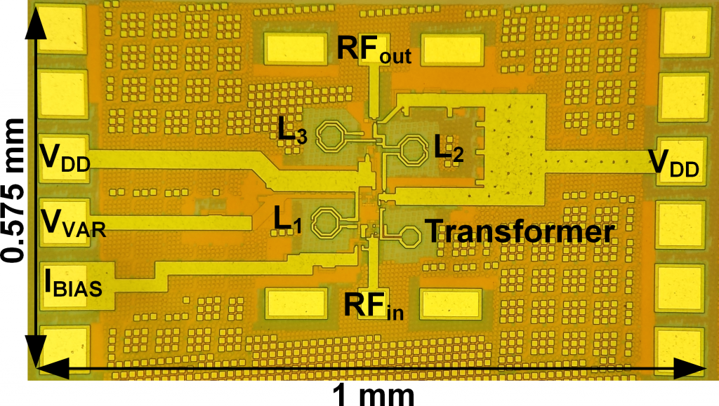
In this work we have designed and implemented a 50-Gb/s transimpedance amplifier (TIA) in a 0.13-μm SiGe BiCMOS process. The proposed TIA, designed for use in a single-channel optical communication network, is comprised of three stages including: 1) a shunt-peaked, shunt-series feedback stage incorporating a transformer-based positive feedback; 2) an RC-degenerated common–emitter stage; and 3) an inductively degenerated emitter follower. The TIA chip integrates an on-chip 100-fF input capacitor to emulate the photo-detector junction capacitor, and achieves a measured transimpedance gain of 41 dB and an input-referred current noise spectral density of 39.8 pA/√Hz over a 50-GHz bandwidth. The TIA achieves an open eye at 50 Gbps with random jitter of 2.3-ps RMS (including the jitter contribution of the test fixture). The prototype chip occupies 0.58 mm2 (including pads) of die area and dissipates 24 mW of dc power from a 2-V supply voltage (i.e., less than 0.5 pJ/bit).
Related Publications:
- Alireza Karimi-Bidhendi, Hossein Mohammadnezhad, Michael M. Green, and Payam Heydari, “A Silicon-Based Low-Power Broadband Transimpedance Amplifier,” in IEEE Transactions on Circuits and Systems: Regular Papers, 2017.
- Hossein Mohammadnezhad, Alireza Karimi Bidhendi, Michael M. Green, and Payam Heydari, “A Low-Power BiCMOS 50 Gbps Gm-Boosted Dual-Feedback Transimpedance Amplifier,” IEEE Bipolar / BiCMOS Circuits and Technology Meeting – BCTM, Boston, MA, 2015, pp. 161-164.
Ultra low-power front-end for brain signal acquisition:
In this research we intend to design a system to enable walking in people suffering from spinal cord inj ury. The purpose of the system is to bypass the damaged nervous system by monitoring/processing the brain signal directly and apply the walking commands to a movement actuator (e.g. exoskeleton). We design low power front-end mixed-signal circuits to acquire brain signals using Electrocorticography (ECoG) method. The signals will be further classified and processed to detect the intention of the subject (walk or not walk) in the system back-end.
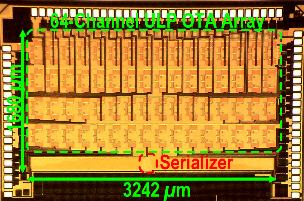
So far, among other works, we have designed two brain signal acquisition (BSA) front-ends incorporating two CMOS ultralow power, low-noise amplifier arrays and serializers operating in MOSFET weak inversion region. To boost the amplifier’s gain for a given current budget, cross-coupled-pair active load topology is used in the first stages of these two amplifiers. These two BSA front-ends are fabricated in 130 and 180 nm CMOS processes, occupying 5.45 mm^2 and 0.352 mm^2 of die areas, respectively (excluding pad rings). The CMOS 130-nm amplifier array is comprised of 64 elements, where each amplifier element consumes 0.216 μW from 0.4 V supply, has input-referred noise voltage (IRNoise) of 2.19 μVRMS corresponding to a power efficiency factor (PEF) of 11.7, and occupies 0.044 mm^2 of die area. The CMOS180 nm amplifier array employs 4 elements, where each element consumes 0.69 μW from 0.6 V supply with IRNoise of 2.3 μV RMS (corresponding to a PEF of 31.3) and 0.051 mm^2 of die area. Noninvasive electroencephalographic and invasive electrocorticographic signals were recorded real time directly on able-bodied human subjects, showing feasibility of using these analog front-ends for future fully implantable BSA and brain– computer interface systems.
Related Publications:
- Alireza Karimi-Bidhendi, Omid Malekzadeh-Arasteh, Mao-Cheng Lee, Colin M. McCrimmon, Po T. Wang, Akshay Mahajan, Charles Yu Liu, Zoran Nenadic, An H. Do, and Payam Heydari, “CMOS Ultralow Power Brain Signal Acquisition Front-Ends: Design and Human Testing,” in IEEE Transactions on Biomedical Circuits and Systems, vol. 11, no. 5, pp. 1111-1122, Oct. 2017.
- Colin McCrimmon, Jonathan Fu, Ming Wang, Lucas Silva Lopes, Po Wang, Alireza Karimi-Bidhendi, Charles Liu, Payam Heydari, Zoran Nenadic, and An Do, “Performance Assessment of a Custom, Portable and Low-Cost Brain-Computer Interface Platform,” in IEEE Transactions on Biomedical Engineering, vol. 64, no. 10, pp. 2313-2320, Oct. 2017.
- Akshay Mahajan, Alireza Karimi Bidhendi, Po T. Wang, Colin M. McCrimmon, Charles Y. Liu, Zoran Nenadic, An H. Do, and Payam Heydari, “A 64-Channel Ultra-Low Power Bioelectric Signal Acquisition System for Brain-Computer Interface,” in IEEE Biomedical Circuits and Systems Conference (BioCAS), Atlanta, GA, 2015, pp.1-4.
A CMOS Inductorless MedRadio OOK Transceiver for Medical Implants
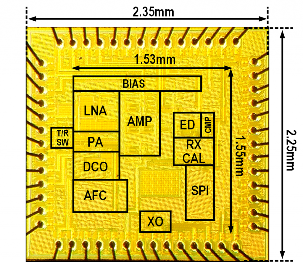
An inductorless MedRadio (413~419 MHz) OOK transceiver for an implantable brain-machine interface in 180 nm CMOS is presented. An event-driven supply modulation technique is introduced in the receiver to lower the power consumption to 42/92 μW at 1/10 kbps, achieving -79/-74 dBm sensitivity (at 0.1% BER). The transmitter employs a current-starved ring oscillator with an automatic frequency calibration loop, achieving 14% efficiency for random OOK data at -4 dBm output power. Wireless connection, benchtop, multi-user coexistence, and in-vitro phantom test results are demonstrated.
Related Publication:
- Mao-Cheng Lee, Alireza Karimi-Bidhendi, Omid Malekzadeh-Arasteh, Po T. Wang, Zoran Nenadic, An H. Do, and Payam Heydari, “A CMOS Inductorless MedRadio OOK Transceiver With a 42μW Event-Driven Supply-Modulated RX and a 14% Efficiency TX for Medical Implants,” IEEE Custom Integrated Circuits Conf. (CICC), April 2018.
- Mao-Cheng Lee, Alireza Karimi-Bidhendi, Omid Malekzadeh-Arasteh, Po T. Wang, An H. Do, Zoran Nenadic and Payam Heydari, “A CMOS MedRadio Transceiver with Supply-Modulated Power Saving Technique for an Implantable Brain-Machine Interface System,” IEEE J. Solid-State Circuits, vol. 54, 2019.
A Fast Start-up Crystal Oscillator
This paper presents a theoretical study and design of two techniques used to reduce start-up time (TS) and energy (ES) of Pierce crystal oscillator (XO). An analytical study of precise injection on a crystal resonator is introduced, and based on this study, a relaxation oscillator with a dithered frequency is designed. Next, a study of negative resistance of XO’s active circuitry and a method to boost its value beyond the limit set by crystal static capacitor are presented. A gyrator-C active inductor with high linearity is developed to accelerate the start-up process by boosting the negative resistance. A prototype integrating these techniques is fabricated in a 180 nm CMOS process, and shows a significant improvement compared to prior art. Specifically, TS and ES are reduced by 102.7 and 2.9, compared to the XO start-up with no assisting circuitry, to 18 s and 114.5 nJ for a 48 MHz XO across -40–90 C temperature range. The measured steady-state power and phase noise of the XO are 180 W and -135 dBc/Hz at 1 kHz offset.
Related Publication:
- Alireza Karimi-Bidhendi, Haoran Pu and Payam Heydari, “Study and Design of a Fast Start-up Crystal Oscillator Using Precise Dithered Injection and Active Inductance,” IEEE J. Solid-State Circuits, vol. 54, 2019.


