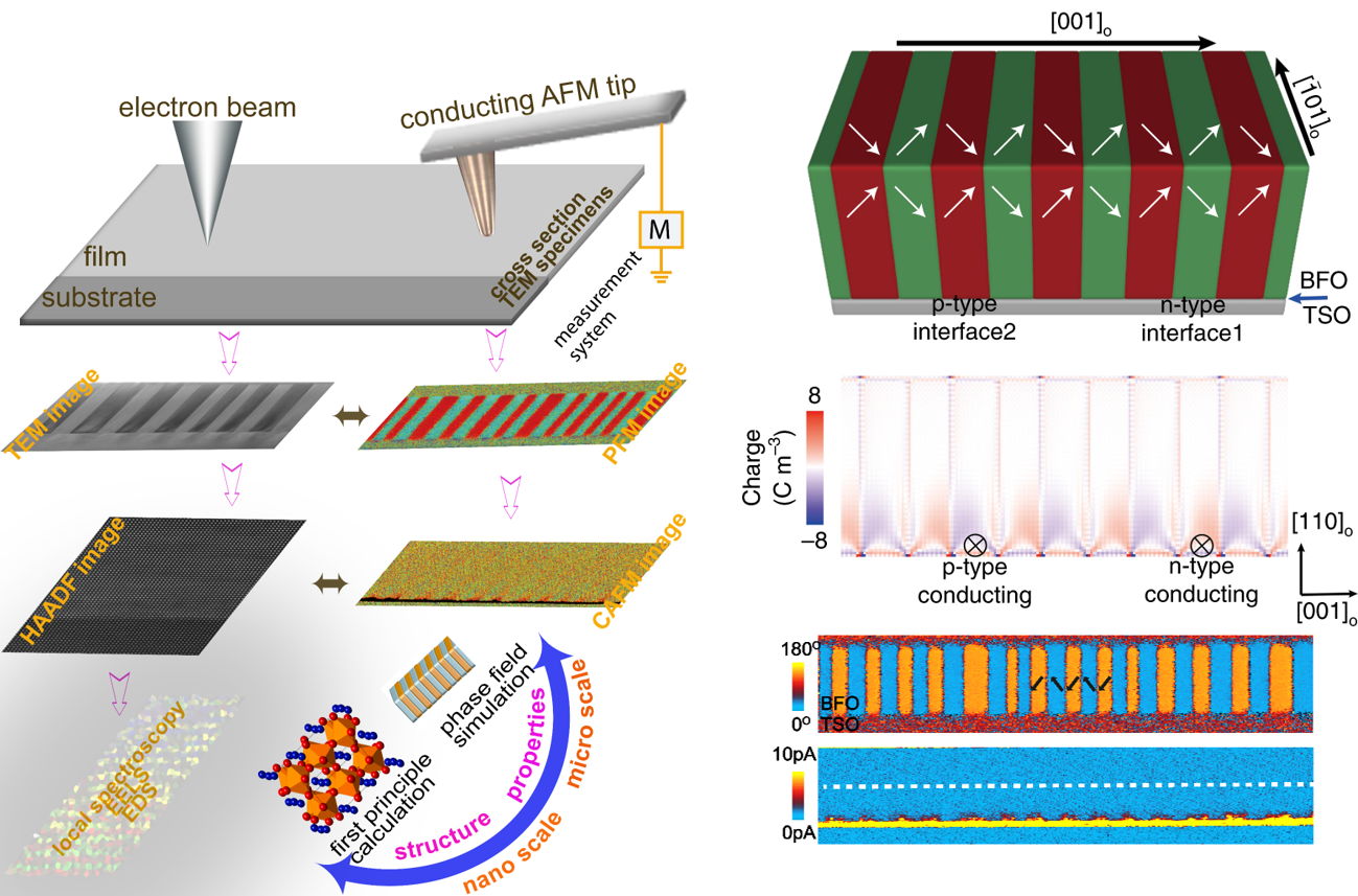
Ferroelectric materials are characterized by a spontaneous electric polarization, which can be reoriented with an applied electric field. The ability to form and manipulate nanoscale regions of uniform polarization (domains) makes ferroelectrics a promising candidate for future low-power electronic devices, particularly computer memories. When ferroelectrics is integrated with other materials, new and unique properties can emerge from interfaces where the two materials join. To understand these emergent properties, it is critical to characterize the atomic structure, chemical bonding, electric field, charge distribution at interfaces. Ferroelectric oxides have become a prototypical example of functional materials, attracting considerable interest in both fundamental research and device engineering. These materials often form domain walls (DWs) which are quasi-2D boundaries separating domains that differ in the orientation of their spontaneous polarization. DWs play an important role in determining many material properties such as stability, conductivity and photovoltaic activity, and they can be created, erased, and reconfigured by external electric fields, making them appealing as active elements in future nanoelectronic devices.
Our group has done extensive studies of the polarization structures in ferroelectric oxides. In 2010, we developed a method of polarization mapping based on atomic displacements in atomic resolution S/TEM images that has become a standard method for measuring polarization. We have applied this method to study a variety of thin film ferroelectrics grown on insulating and conducting substrates. We also use specialized in-situ TEM probe holders to study the dynamics of domain switching in ferroelectrics and applying 4D STEM to ferroelectrics.
One of our current projects is charge separation across 109 degree domain walls in BiFeO3. At the domain wall, we observed a displacement discontinuity that may induces unbalanced charge in the local DW area because the weaker polarization dipole at the DW is not able to fully compensate the negative and positive charge that is produced by the dipoles in the two adjacent unit cells, respectively. This was observed by atomic resolution imaging and low convergence angle 4D STEM.


Related Publications
- Gao, W., Addiego, C., Wang, H., Yan, X., Hou, Y., Ji, D., Heikes, C., Zhang, Y., Li, L., Huyan, H., Blum, T., Aoki, T., Nie, Y., Schlom, D.G., Wu, R., Pan, X.Q., Real-Space Charge-Density Imaging with Sub-Angstrom Resolution by Four-Dimensional Electron Microscopy. Nature 2019 575, 490-484. https://doi.org/10.1038/s41586-019-1649-6
- Li, L., Cheng, X., Jokisaari, J. R., Gao, P., Britson, J., Adamo, C., Heikes, C., Schlom, D. G., Chen, L. Q., Pan, X., Defect-Induced Hedgehog Polarization States in Multiferroics. Physical Review Letters 2018, 120 (13), 137602. https://doi.org/10.1103/PhysRevLett.120.137602
- Zhang, Y., Lu, H., Xie, L., Yan, X., Paudel, T. R., Kim, J., Cheng, X., Wang, H., Heikes, C., Li, L., Xu, M., Schlom, D. G., Chen, L. Q., Wu, R., Tsymbal, E. Y., Gruverman, A., Pan, X., polarization-induced conductance at a ferroelectric–insulator interface. Nature Nanotechnology 2018, 13 (12), 1132-1136. https://doi.org/10.1038/s41565-018-0259-z
- C.T. Nelson, P. Gao, J. Jokisaari, C. Heikes, C. Adamo, A. Melville, S.H. Baek, C.M. Folkman, B. Winchester, Y.G. Gu, Y.M. Liu, K. Zhang, E. G. Wang, J.Y. Li, L.Q. Chen, C.B. Eom, D.G. Schlom, and X.Q. Pan, “Domain Dynamics during Ferroelectric Switching,” Science, Vol. 334, Issue 6058, pp. 968-971 (2011).
- C.T. Nelson, B. Winchester, Y. Zhang, S.J. Kim, A. Melville, C. Adamo, C.M. Folkman, S.H. Baek, C.B. Eom, D.G. Schlom, L.Q. Chen, and X.Q. Pan, “Spontaneous Vortex Nanodomain Arrays at Ferroelectric Hetero-Interfaces,” Nano Letters, Vol. 11, Issue 2, pp. 828-834 (2011).


