Single-defect phonons imaged by electron microscopy
X. Yan et al., Nature 589, 65–69 (2021)

Crystal defects affect the thermal and heat-transport properties of materials by scattering phonons and modifying phonon spectra. To appreciate how imperfections in solids influence thermal conductivity and diffusivity, it is thus essential to understand phonon–defect interactions. Sophisticated theories are available to explore such interactions, but experimental validation is limited because most phonon-detecting spectroscopic methods do not reach the high spatial resolution needed to resolve local vibrational spectra near individual defects. Here we demonstrate that space- and angle-resolved vibrational spectroscopy in a transmission electron microscope makes it possible to map the vibrational spectra of individual crystal defects. We detect a red shift of several millielectronvolts in the energy of acoustic vibration modes near a single stacking fault in cubic silicon carbide, together with substantial changes in their intensity, and find that these changes are confined to within a few nanometres of the stacking fault. These observations illustrate that the capabilities of a state-of-the-art transmission electron microscope open the door to the direct mapping of phonon propagation around defects, which is expected to provide useful guidance for engineering the thermal properties of materials.
Real-space charge-density imaging with sub-ångström resolution by four-dimensional electron microscopy
W. Gao, C. Addiego, H. Wang et al., Nature 575, 480–484 (2019)

The distribution of charge density in materials dictates their chemical bonding, electronic transport, and optical and mechanical properties. Indirectly measuring the charge density of bulk materials is possible through X-ray or electron diffraction techniques by fitting their structure factors, but only if the sample is perfectly homogeneous within the area illuminated by the beam. Meanwhile, scanning tunnelling microscopy and atomic force microscopy enable us to see chemical bonds, but only on the surface. It remains a challenge to resolve charge density in nanostructures and functional materials with imperfect crystalline structures—such as those with defects, interfaces or boundaries at which new physics emerges. Here we describe the development of a real-space imaging technique that can directly map the local charge density of crystalline materials with sub-ångström resolution, using scanning transmission electron microscopy alongside an angle-resolved pixellated fast-electron detector. Using this technique, we image the interfacial charge distribution and ferroelectric polarization in a SrTiO3/BiFeO3 heterojunction in four dimensions, and discover charge accumulation at the interface that is induced by the penetration of the polarization field of BiFeO3. We validate this finding through side-by-side comparison with density functional theory calculations. Our charge-density imaging method advances electron microscopy from detecting atoms to imaging electron distributions, providing a new way of studying local bonding in crystalline solids.
Anisotropic polarization-induced conductance at a ferroelectric-insulator interface
Y. Zhang et al., Nature Nanotech 13, 1132–1136 (2018)
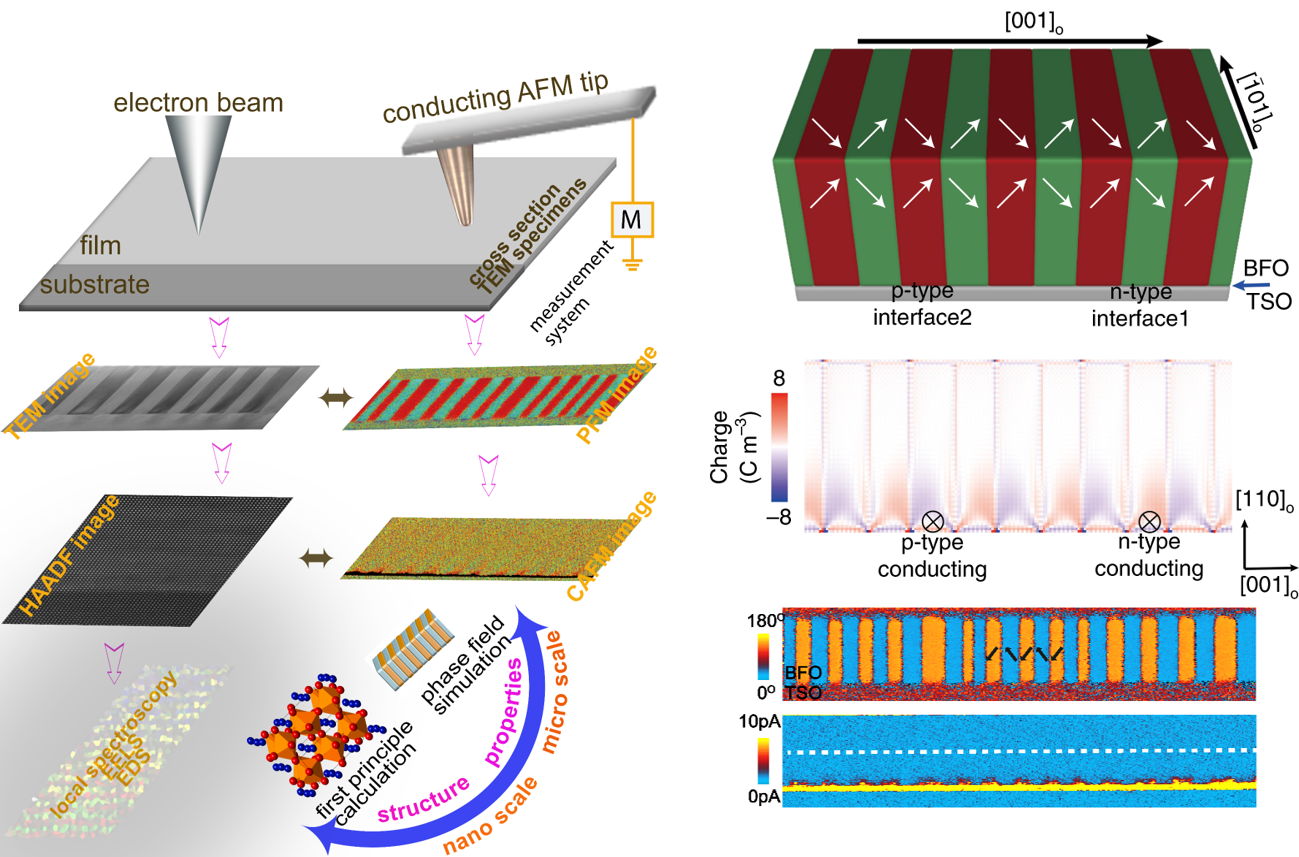
Coupling between different degrees of freedom, that is, charge, spin, orbital and lattice, is responsible for emergent phenomena in complex oxide heterostrutures. One example is the formation of a two-dimensional electron gas (2DEG) at the polar/non-polar LaAlO3/SrTiO3 (LAO/STO) interface. This is caused by the polar discontinuity and counteracts the electrostatic potential build-up across the LAO film. The ferroelectric polarization at a ferroelectric/insulator interface can also give rise to a polar discontinuity. Depending on the polarization orientation, either electrons or holes are transferred to the interface, to form either a 2DEG or two-dimensional hole gas (2DHG). While recent first-principles modelling predicts the formation of 2DEGs at the ferroelectric/insulator interfaces, experimental evidence of a ferroelectrically induced interfacial 2DEG remains elusive. Here, we report the emergence of strongly anisotropic polarization-induced conductivity at a ferroelectric/insulator interface, which shows a strong dependence on the polarization orientation. By probing the local conductance and ferroelectric polarization over a cross-section of a BiFeO3–TbScO3 (BFO/TSO) (001) heterostructure, we demonstrate that this interface is conducting along the 109° domain stripes in BFO, whereas it is insulating in the direction perpendicular to these domain stripes. Electron energy-loss spectroscopy and theoretical modelling suggest that the anisotropy of the interfacial conduction is caused by an alternating polarization associated with the ferroelectric domains, producing either electron or hole doping of the BFO/TSO interface.
Spontaneous vortex nanodomain arrays at ferroelectric heterointerfaces
C.T. Nelson et al., Nano Lett. 11, 828–834 (2011)

The polarization of the ferroelectric BiFeO3 sub-jected to different electrical boundary conditions by heterointerfaces is imaged with atomic resolution using a spherical aberration-corrected transmission electron microscope. Unusual triangular-shaped nanodomains are seen, and their role in providing polarization closure is understood through phase-field simulations. Heterointerfaces are key to the performance of ferroelectric devices, and this first observation of spontaneous vortex nanodomain arrays at ferroelectric heterointerfaces reveals properties unlike the surrounding film including mixed Ising−Néel domain walls, which will affect switching behavior, and a drastic increase of in-plane polarization. The importance of magnetization closure has long been appreciated in multidomain ferromagnetic systems; imaging this analogous effect with atomic resolution at ferroelectric heterointerfaces provides the ability to see device-relevant interface issues. Extension of this technique to visualize domain dynamics is envisioned.
Domain dynamics during ferroelectric switching
C.T. Nelson et al., Science 334, 968-971 (2011)

The utility of ferroelectric materials stems from the ability to nucleate and move polarized domains using an electric field. To understand the mechanisms of polarization switching, structural characterization at the nanoscale is required. We used aberration-corrected transmission electron microscopy to follow the kinetics and dynamics of ferroelectric switching at millisecond temporal and subangstrom spatial resolution in an epitaxial bilayer of an antiferromagnetic ferroelectric (BiFeO3) on a ferromagnetic electrode (La0.7Sr0.3MnO3). We observed localized nucleation events at the electrode interface, domain wall pinning on point defects, and the formation of ferroelectric domains localized to the ferroelectric and ferromagnetic interface. These results show how defects and interfaces impede full ferroelectric switching of a thin film.